The BPCMCIA peripheral board attached to provides a standard PCMCIA interface for SRAM cards. It addresses PCMCIA devices of up to 8 Mb in size.
The BPCMCIA may be mapped into either the memory or I/O space of an SBC2000. When memory mapping is selected, a 128k window is used for access to the SRAM device. When I/O space mapping is selected, a 32k window is used for access to the SRAM device.
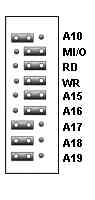
1. Set jumpers as follows:
2. Install the BPCMCIA on SBC2000 and insert a SRAM card.
3. Execute the following code:
	GLOBAL i AS INTEGER
CONSTANT crlf AS STRING = "\013\010"

REM Use first 128K of SRAM card
CALL iopoke(0x0000,0x00)

REM Write and Dump the first 10 locations
FOR i = 0 TO 9
	mem_poke(i, i)
	PRINT mem_peek(i), crlf
NEXT i
The region of PCMCIA space that is currently addressable is selected by writing to an I/O register the top six bits of the 23-bit PCMCIA address. (The top eight bits are written in the case of I/O space mapping). This register resides at I/O address 0x0000 or 0x0400. Select this register with jumper A10:
| A10 | PCMCIA Base Register Address |
| 2-3 | shorted 0X0000 in IO space |
| 1-2 | shorted 0X0400 in IO space |
Select memory and I/O mapping with five jumpers (M/IO, RD, WR, A15 and A16), as follows.
| MEMIO Jumpers | Mapping |
| 2-3 | shorted IO Space |
| 1-2 | shorted Memory Space |
The 32k IO space region always resides in the 32k region of IO space, starting at offset 0x8000.
| Pin | Signal | Pin | Signal | Notes |
| 1 | GND | 35 | GND | |
| 2 | D3 | 36 | CD1 | CD1 is used with CD2 to detect card insertion |
| 3 | D4 | 37 | n.c. | |
| 4 | D5 | 38 | n.c. | |
| 5 | D6 | 39 | n.c. | |
| 6 | D7 | 40 | n.c. | |
| 7 | CE1* | 41 | n.c. | CE1 is asserted whenever an address within the SBC2000 window is selected |
| 8 | A10 | 42 | CE2 | CE2 is tied high to keep SRAM cards in8-bit mode. |
| 9 | RD* | 43 | n.c. | |
| 10 | A11 | 44 | n.c. | |
| 11 | A9 | 45 | n.c. | |
| 12 | A8 | 46 | A17 | |
| 13 | A13 | 47 | A18 | |
| 14 | A14 | 48 | A19 | |
| 15 | WR* | 49 | A20 | |
| 16 | n.c. | 50 | A21 | |
| 17 | +5V | 51 | +5V | |
| 18 | n.c. | 52 | n.c. | |
| 19 | A16 | 53 | A22 | |
| 20 | A15 | 54 | n.c. | |
| 21 | A12 | 55 | n.c. | |
| 22 | A7 | 56 | n.c. | |
| 23 | A6 | 57 | n.c. | |
| 24 | A5 | 58 | RESET | RESET is asserted only at powerup. |
| 25 | A4 | 59 | WAIT | WAIT is connected directly to the BUS WAIT pin (J1A-10). |
| 26 | A3 | 60 | n.c. | |
| 27 | A2 | 61 | REG | |
| 28 | A1 | 62 | BVD1 | |
| 29 | A0 | 63 | BVD2 | |
| 30 | D0 | 64 | n.c. | |
| 31 | D1 | 65 | n.c. | |
| 32 | D2 | 66 | n.c. | |
| 33 | WP | 67 | CD2 | WP (Write Protect switch position) is ignored |
| 34 | GND | 68 | GND | |
The battery voltage detect functions are not supported.
Readout of the configuration register on an SRAM is not supported.
| Pin | Signal | Pin | Signal |
| J1A-1 | N.C. | J1B-1 | GND |
| J1A-2 | D7 | J1B-2 | N.C. |
| J1A-3 | D6 | J1B-3 | +5V |
| J1A-4 | D5 | J1B-4 | N.C. |
| J1A-5 | D4 | J1B-5 | N.C. |
| J1A-6 | D3 | J1B-6 | INT* |
| J1A-7 | D2 | J1B-7 | N.C. |
| J1A-8 | D1 | J1B-8 | N.C. |
| J1A-9 | D0 | J1B-9 | N.C. |
| J1A-10 | N.C. | J1B-10 | GND |
| J1A-11 | AEN | J1B-11 | N.C. |
| J1A-12 | A19 | J1B-12 | N.C. |
| J1A-13 | A18 | J1B-13 | IOW |
| J1A-14 | A17 | J1B-14 | IOR |
| J1A-15 | A16 | J1B-15 | N.C. |
| J1A-16 | A15 | J1B-16 | N.C. |
| J1A-17 | A14 | J1B-17 | N.C. |
| J1A-18 | A13 | J1B-18 | N.C. |
| J1A-19 | A12 | J1B-19 | N.C. |
| J1A-20 | A11 | J1B-20 | N.C. |
| J1A-21 | A10 | J1B-21 | N.C |
| J1A-22 | A9 | J1B-22 | N.C |
| J1A-23 | A8 | J1B-23 | N.C. |
| J1A-24 | A7 | J1B-24 | IRQ4 |
| J1A-25 | A6 | J1B-25 | IRQ3 |
| J1A-26 | A5 | J1B-26 | N.C. |
| J1A-27 | A4 | J1B-27 | N.C. |
| J1A-28 | N.C. | J1B-28 | ALE |
| J1A-29 | A2 | J1B-29 | +5V |
| J1A-30 | A1 | J1B-30 | N.C. |
| J1A-31 | A0 | J1B-31 | N.C. |
| J1A-32 | GND | J1B-32 | GND |
The amount of current drawn by a BPCMCIA with an SRAM card installed is 16 mA.
Dimensions are in inches.